





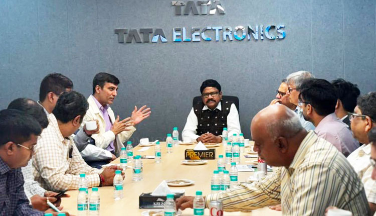
Bhubaneswar: With an aim to strengthen modern technology and industrial infrastructure in Odisha and create a conducive environment for the semiconductor industry, Electronics and IT Minister Dr Mukesh Mahaling visited Dholera in Gujarat.
During the visit, detailed discussions were held on integrated infrastructure and urban development in Dholera and the activation area was inspected. The Minister took note of the modern urban planning and extensive infrastructure development that has been undertaken in Dholera, which were the main attractions of the visit.
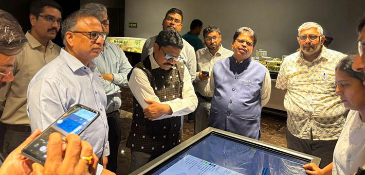
Dr Mahalinga also visited Tata Electronics’ semiconductor fab in Dholera. He observed that the development of the semiconductor industry is not limited to setting up a fab alone, but also requires building the necessary industry ecosystem, vendor network, high-quality infrastructure and skilled human resources.
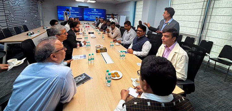
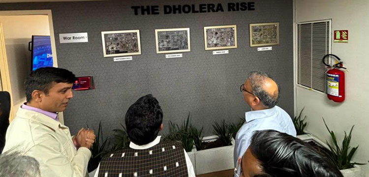 Speaking on the occasion, the Minister said the visit has provided valuable experience and learnings for building the future semiconductor ecosystem in Odisha. “Under the guidance of Prime Minister Narendra Modi and the leadership of Chief Minister Mohan Charan Majhi, Odisha is all set to become the future semiconductor and technology hub of India through a combination of modern infrastructure, advanced technology and industry ecosystem,” he said.
Additional Chief Secretary of Electronics and IT Department Vishal Dev, OPTCL Chairman Bhaskar Jyoti Sharma, OCAC CEO Dr Pradeep Kumar Raut, Joint Secretary Kaustuva Pany and other senior officials accompanied the Minister during the visit.